
Formula is a revision of a module I called Ffrydiau, a two stage ‘wave distortion’ module which in turn was based on the ‘Simple Wavefolder’ or CGS52 by Ken Stone (Stone derived this from a circuit described by R.Lockhart Junior, sometimes referred to as the Lockhart Wavefolder). Formula is an update to Ffrydiau, aiming to simplify the circuit concept and to focus on the best features. This module builds upon Stone’s Simple Wavefolder concept, it has a VCA frontend which allows for voltage control to modulate the effect and has two seperate stages which produces a more extreme sonic effect. As the effect sounds quite different at each stage, individual outputs are provided. A third output mixes the input signal with the processed signal, with the processed signal out of phase so as to avoid clipping . Other than the main CV input, there is an ‘Offset’ input which accepts a second waveform, applying an LFO to the offset input is ideal, and between this and CV control a variety of sonic effects can be produced. The concept of this module is to produce a harmonically rich waveform from a harmonically simple waveform (e.g. a sine or triangle wave), in some regards it is the opposite of a filter. There is AC coupling as part of the core circuit, so this module is really designed for audio rate signals, slow modulation signals are not likely to work so well.
This module creates exotic and harmonically rich sounds. There are two distortion stages based on BJT push-pull amplifiers. Normally this kind of amplifier will utilise a negative feedback path to avoid cross-over distortion, but this circuit makes a feature out of this ‘undesired’ non-linear effect. Because the distortion is the result of the input waveform in the push-pull cross-over region, applying a DC offset to the signal can produce some very interesting effects. I have found that a triangle wave signal input with a triangle LFO applied to the Offset input can create a sound like multiple detuned sawtooths playing together, there is lots to explore!
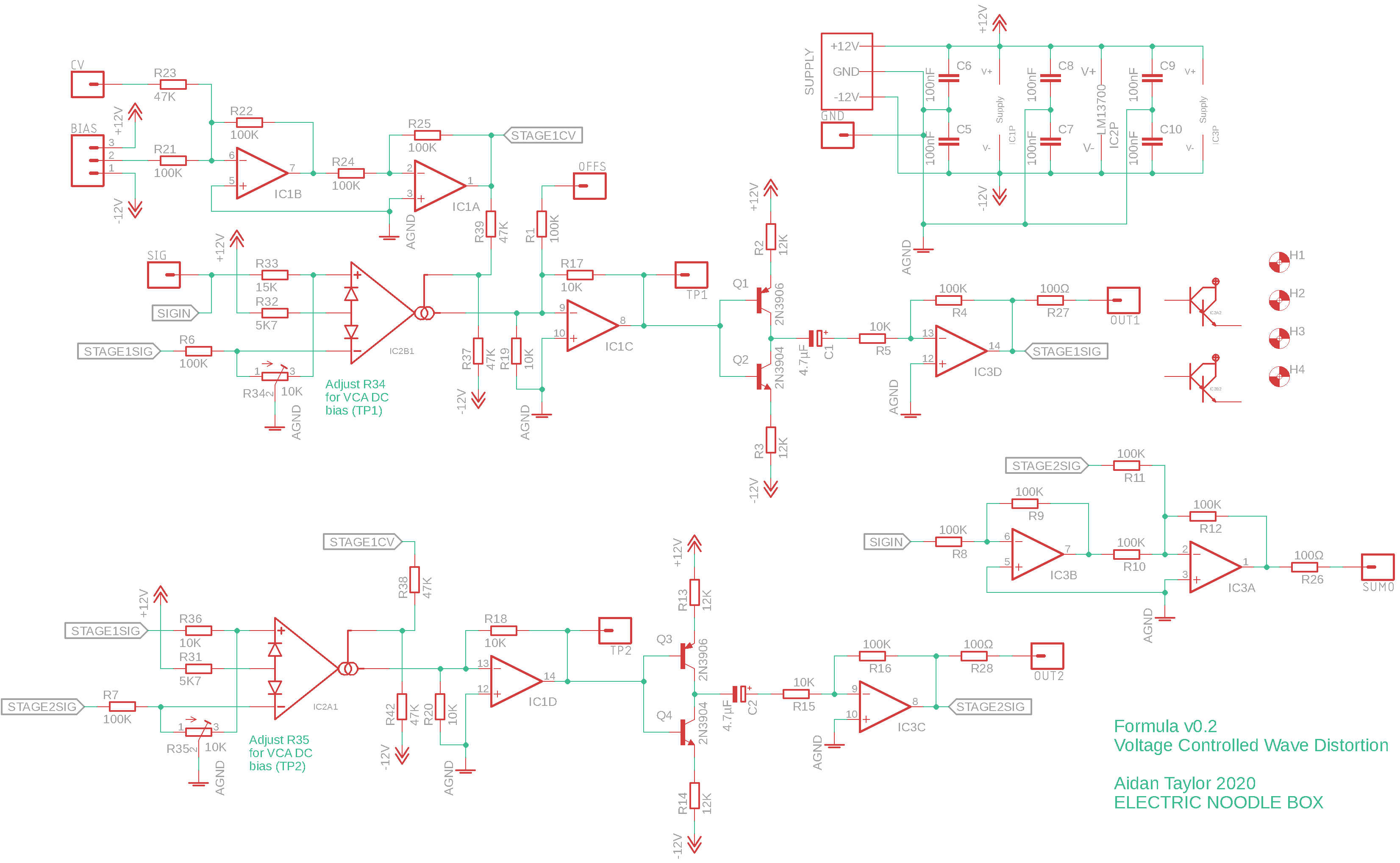
A detailed description of the way this circuit works is included at the bottom of this page.
You can purchase a good quality PCB from me which has already been tried and tested through design revisions to work as described – coming soon
Hint: you can right click and select “View Image” to blow it up, alternatively there is a .pdf included in the repository:
View the schematic in the repository
Specifics:
- Supply Voltage: ±12V Supply
- Supply Current: TBA
- Inputs: Main signal input should be ramping (sine, saw, triangle) audio signal at ±5V, CV is intended to be in the 0-10V range but negative going signals will not hurt and you can set for this using the Bias control. Offset input can be pretty much anything, but I would suggest applying signals in the ±5V range.
- Outputs: Outputs are typically ±5V but applying the distortion can push it to a greater amplitude, this is unlikely to be a problem within the ENB modular system, but you might want to consider this for connecting to external gear.
Building
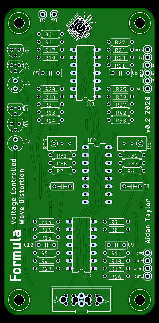
Resistor numbers are found on top of the part due to the small amount of available space, this means that it can be hard to locate a part if you have soldered up the PCB – use the image below to help locate parts.
There is a layout to scale available as a printable .pdf in the repository. This image also includes the routing on the PCB so may be helpful if you need to diagnose faults.
View the bill of materials here
This circuit can definitely be constructed on breadboard for testing, but it is a large design so I would recommend using two full size breadboards and to spread out the chips to allow yourself space to work. You will need a ±12V power supply at very least for testing.
I would recommend using 10K-100K potentiometers configured as an attenuator to ground for CV inputs – which will allow control over modulation depth. See the image for control wiring (right click and select ‘view image’ to blow it up):
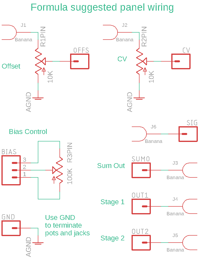
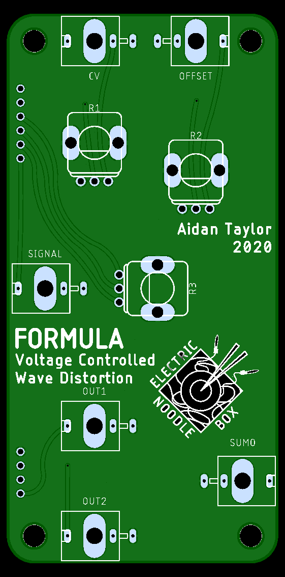
A control PCB and front panel is also available (coming soon) – this is Eurorack panel size standard, and can take either banana sockets or mini-jacks. Be aware that the banana sockets are specifically intended to be Cinch type, as these have a good vertical depth that matches the potentiometers used. The mini-jack footprint is for the PJ398SM (Thonkiconn) sold by Thonk. Link to BOM below.
Layout (printable to scale)
Calibration
The two VCAs in this design have a trimmer to adjust for DC bias in the output. As Iabc (current to amplifier bias pin on LM13700) increases, the output becomes slightly positively biased. To correct for this, you ideally need an oscilloscope to monitor the output. Make sure the oscilloscope is set to DC mode and connect the probe to TP1 or TP2 to check the bias of the two stages. Apply a sine wave to the input that is known to be correctly centered. Set the bias control to maximum, or alternatively apply a 10V DC signal to the CV input. Adjust trimmer R34 or R35 so that the output signal is centred around 0V. Do this for each amplifier stage. There is normally a tiny amount of DC bias when the VCA is closed, this will be cancelled out by the AC coupling following the push-pull amplifier stage.
A note on the output – the transistors that make up the push-pull amplifiers are pairs of NPN and PNP types, so cannot easily be matched. This means that the crossover distortion effect, which is the desired sonic effect in this design, will likely look different on the scope and sound different for any set of transistors used. It might be possible to match transistors for Hfe to get more replicatable results, however I have not aimed for linearity in this design (I may explore it further in the future) because I think it sounds great regardless, I have tried swapping out transistors on the fly and it never ‘breaks’ the circuit. So the intention is to correctly bias the signal for DC offset at the VCA stage, and have the option to inject a DC offset with the specified input to do so, which creates interesting sonic effects. I definitely have an ‘if it ain’t broken, don’t fix it’ attitude here, but would welcome any suggestions on improving balance post push-pull amplifier stage and/or replicability. I think you will enjoy using this circuit regardless!
Circuit Description
I recommend that you keep a copy of the schematic to hand when following this description.
This module has a few simple sections, a linear VCA pair based on the LM13700 which share a CV input and the push-pull amplifiers which connect to a simple op-amp summing stage.
IC2 is an LM13700 chip, both amplifiers on this chip are used to make a simple voltage controlled amplifier, IC2A and IC2B in the schematic. The input to the LM13700 is suitably high impedance for audio, but the output is a current that needs buffering – I generally favour using a high-impedance input op-amp over the on-chip Darlington buffers provided with the LM13700, this is the purpose of IC1C and IC1D which are two amplifiers of a TL084. Note that IC1C and IC1D are both inverting amplifiers, so the input signal will be 180º out of phase following the VCA circuit block. Note that the linearising diodes are used in this design to prevent non-linear distortion of the input, R32 and R31 apply a biasing current to the internal diodes (this is pretty funny when you consider what happens to the signal following this stage!). Also note the trimmer across the inputs of each VCA, R34 and R35. As control current is increased to open the amplifier, the output tends to get positively biased – the trimmer is used to calibrate the LM13700 to counteract this.
IC2A and IC2B both have gain set by current applied to the ‘amplifier bias pin’ (Iabc), the pin is biased to the negative supply rail which is -12V, and will open the amplifier based on how much it is allowed to sink current. CV and a DC bias control are applied to the module to control the VCAs. I used quite a simple configuration using op-amps to make a linear control, see IC1B which is a summing inverting amplifier and IC1A which is a second inverting amplifier. Both amplifiers are set to unity gain and the inputs to IC1B are split between a potentiometer to set a DC bias and an input for an external CV signal. The output of this op-amp pair will not exceed the supply rail at +12V and they will likely saturate before this. The current control for the LM13700 amplifier bias pins is protected by R39 and R38 based on a +12V peak as a worst case scenario (using ohms law, 24V differential and limiting Iabc to 1ma: R=E/I = 24000 or 24K, but actually R39 and R38 are 47K which will limit current even further). Note that the current source is shared by both VCAs. I found that a second resistor from the amplifier bias pin to the negative rail was helpful in setting the active range of the amplifier, and ensuring it will close fully, this is the purpose of R37 and R42. I want to make a note here that I think this current source is a bit ‘hacky’, in a future revision I will probably design something similar to the circuit used in all of my other LM13700 circuits.
The output of IC1C and IC1D connects to a push-pull amplifier made up by an NPN – PNP transistor pair where the two transistors share a base voltage and have linked collectors. This is a useful configuration for a number of buffer and amplifier applications, but is subject to ‘cross-over distortion’. Normally, cross-over distortion is countered using negative feedback in some form, but this circuit exploits this characteristic for a sonic effect. The cross-over region is a small window in ± voltage around 0V, as the signal increases in amplitude, the output waveform is a representation of the input, only folding over on itself. Sonically, the output will be similar to the input, but with a richer set of harmonics (a flute tone would sound more like a oboe for example). If the signal exceeds this window however, the output will follow the input more accurately. R17 and R18 are feedback resistors which set the gain of the buffer amplifiers for the VCAs, and reduce the signal suitably to work within the crossover region, where the interesting stuff is happening. The push-pull amplifiers made up by Q1 and Q2 for stage 1, and Q3 and Q4 for stage 2, tend to create a DC offset which I think is down to the imperfect matching of the transistor pair – again this would normally be ‘fixed’ with a negative feedback path. I found that matching transistors for Hfe (some multimeters can do this, but don’t worry if you are not able to), AC coupling and a feedback path to the input of the VCA improved on this bias – again this feels a bit ‘hacky’, but who is complaining?!
Finally, the output of each push-pull stage is buffered and re-amplified to modular signal levels by IC3D and IC3C which are configured as inverting amplifiers (correcting the 180º phase of the VCA output). IC3D and IC3C are broken out to patch points so the effect can be used, but I also use another pair of op-amps (IC3B and IC3A) to create a mix output which includes the original signal. The effected output from stage 2 is summed at a phase of 180º with the original input, which I found was better for amplitude and sonic effect.
That’s all for now, happy patching!
