
I am no longer developing this module, it functions as described but I had some mechanical issues in construction and Transients is replacing Knives as a multi-function envelope for the ENB Modular system. There is still plenty of useful information on this page so I will maintain it for your study.
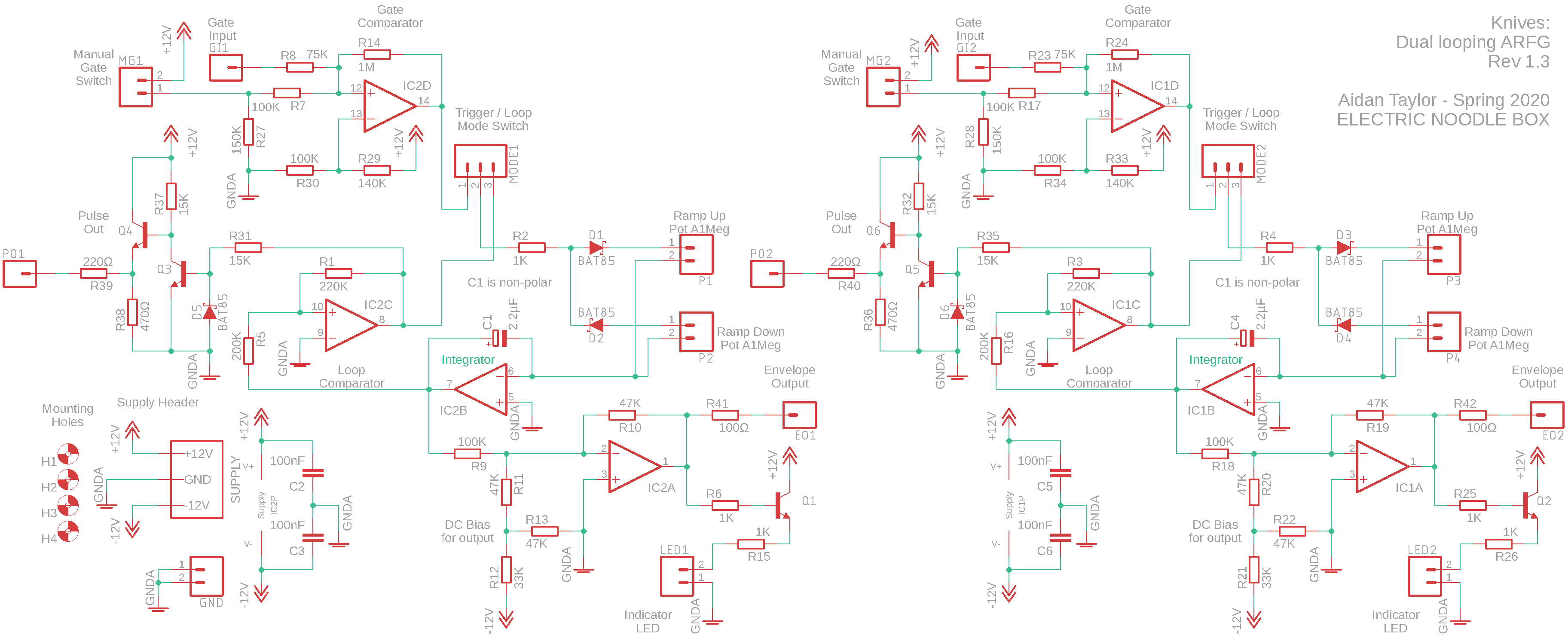
This page describes a DIY envelope or function generator project. This design is similar to the LFO in my Turbo synth project, which was a simple relaxation oscillator built with a TL072 op-amp. This design uses a single TL084 and adds a number of additional features to the original, such as a trigger mode for single cycles. The circuit is simple so it is easy to fit two duplicates on a single PCB, on veroboard or on a breadboard. It works in an interesting responsive way as an envelope, and can be considered as being Attack Hold Release (AHR) configuration. When the gate input is high, the output will ramp up from 0V until the gate input goes low or the output reaches 10V. When the gate is low the output will ramp down until reaching 0V unless a high gate is applied. The ramp up and ramp down times are set by a pair of potentiometers and a switch will set the function into looping mode where it will behave more like an LFO.
A detailed description of the circuit is included at the bottom of this page.
You can purchase a good quality PCB from me which has already been tried and tested through design revisions to work as described – coming soon
Hint: right click and select “View Image” to blow it up, you might find the link below is better again:
View the schematic in the repository
Specifics:
- Supply Voltage: ±12V Supply
- Supply Current: 32mA +12V rail, 25mA -12V rail
- CV/Gate Input to trigger function: Off < 5V > On
- Function Output: 0V – 10V
Building:
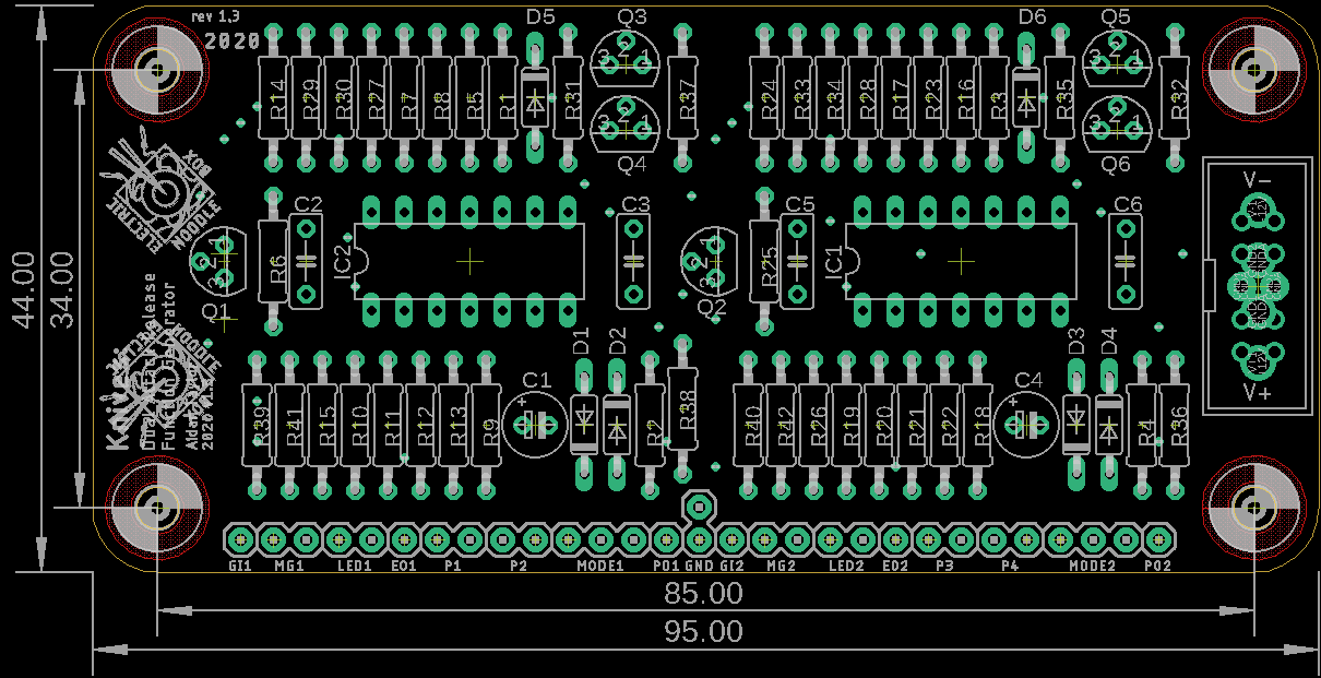
Resistor numbers are found on top of the part due to the small amount of available space, this means that it can be hard to locate a part if you have soldered up the PCB – use the image below to help locate parts.
There is a .pdf with the layout to scale here
This circuit can definitely be constructed on breadboard for testing, use a full size breadboard and spread out the three chips to allow yourself space to work. You will need a ±12V power supply for testing.
View the bill of materials here
Note that the bill of materials should be taken as a guideline only. The BOM has some suggestions for panel wiring if you are building from the core PCB or on veroboard.
The diagram below shows a suggested panel wiring configuration (right click and select ‘view image’ to blow it up):
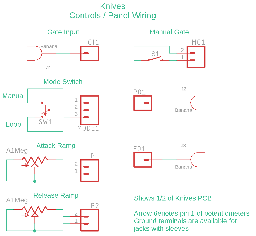
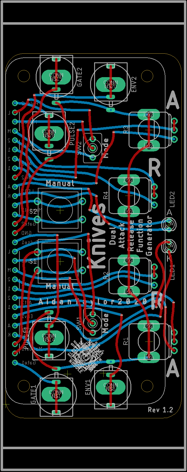
A control PCB and front panel is also available (coming soon) – this is Eurorack panel size standard, and can take either banana sockets or mini-jacks. Be aware that the banana sockets are specifically intended to be Cinch type, as these have a good vertical depth that matches the potentiometers used. The mini-jack footprint is for the PJ398SM (Thonkiconn) sold by Thonk. Link to BOM below.
Layout (to scale)
Circuit Description:
The schematic shows two identical copies of the same circuit, so it is only necessary to describe one half. I recommend that you keep a copy of the schematic available to follow this description.
This circuit features an op-amp configured as an integrator which works in response to one of two op-amps configured as comparators, selected by a mechanical switch. An integrator is an op-amp with a capacitor placed in the negative feedback path, as is the case with IC2B. The incoming voltage is connected to the inverting input of this amplifier which means the op-amp will try to balance out by setting the output to swing the opposite way. C1 will need to charge in order for IC2B to reach a balanced state, which results in a slow ramping voltage. C1 is a 2.2µF non-polarised electrolytic in my design which gives a nice balance between snappy envelopes for dynamics and longer ramps for sweeping modulations. A smaller capacitor will take less time to charge and a larger capacitor will take more time. There is a trade off when selecting a capacitor, larger capacitors will produce longer ramps, but will make it harder to dial in fast dynamics – if you want to adjust the range and decide to use a different electrolytic, make sure it is a non-polar type. Stepping back a little further in the circuit, notice that the input is linked through a pair of 1M potentiometers. These are in parallel but each has a series Schottky diode facing the opposite way. Each Schottky diode will only allow current to travel in one direction, forcing C1 to charge and discharge via one of the two potentiometers. The potentiometer resistance sets the charge rate – so in combination D1 and Pot1 set the ramp up time and D2 and Pot2 set the ramp down time. This circuit block could make an interesting slew control for CV processing. One final note about the potentiometers is that they are logarithmic taper types, I found that this felt more natural for adjusting ramp times than standard linear tapers.
The input signal to the integrator section comes from one of two comparators, selected by a mechanical switch. With the mode switch in the first position, IC2D is selected. IC2D is intended for either a manual switch or an external gate signal to trigger a single cycle of the envelope. The comparator has a threshold of 5V set by the voltage divider made up by R29 and R30, linked to the inverting input. This means that if the voltage at the non-inverting input is greater than 5V, IC2D will output in high saturation, close to the positive supply rail. If the voltage is below 5V then IC2D will output in low saturation, close to the negative supply. Resistor R27 is connected to 0V and this will normally keep IC2D in low saturation. Either pressing the button or inputing a high gate or other signal to the non-inverting input will cause the comparitor to change state. If you follow the signal path you should get an impression of how this will interact with the integrator.
IC2C is a comparator with the threshold set at 0V. The input to IC2C comes directly from the integrator and if the mode switch is set in the opposite position, the output of IC2C links back in to the integrator section. Because IC2B inverts the input signal, this will result in an oscillation as comparator and integrator will continously work against each other; the comparator flips states when the ramp hits a set threshold and the ramp will always work away from the comparator state. Resistor R1 sets a wide hysterisis to the threshold detection in IC2C, which in turn sets the overall voltage swing of IC2B. This mode works as a looping function or an LFO with shape control set by the potentiometers.
An output is also broken out from comparator IC2C which can be used as a gate pulse to control something else – such as the other function generator in this circuit. This output is inverted and buffered using a pair of BJT NPN transistors. Q3 is configured as a ‘NOT’ gate and Q4 is a common collector amplifier. The negative end of the signal input to Q3’s base is clipped by D5 to prevent IC2C pulling the voltage too low for the base-emitter junction, which would destroy the transistor. The output should be a clean 0-10V pulse in any operating mode of the function generator.
The output of IC2B swings above and below 0V, and will also ramp the opposite way to the trigger input from IC2D, which is not normally the intention of an envelope. So the last amplifier on the TL084 chip, IC2A, is configured as an inverting amplifier to bring the signal into the modulation range of 0-10V. The signal is attenuated as R9 and R10 will result in the op-amp gain being close to *0.5. A DC bias set by R13 and R12 and is summed in to set the amplifier output in the positive voltage range. An indicator LED is set to this main output using a 2N3904 NPN transistor configured as a common collector voltage follower.
