
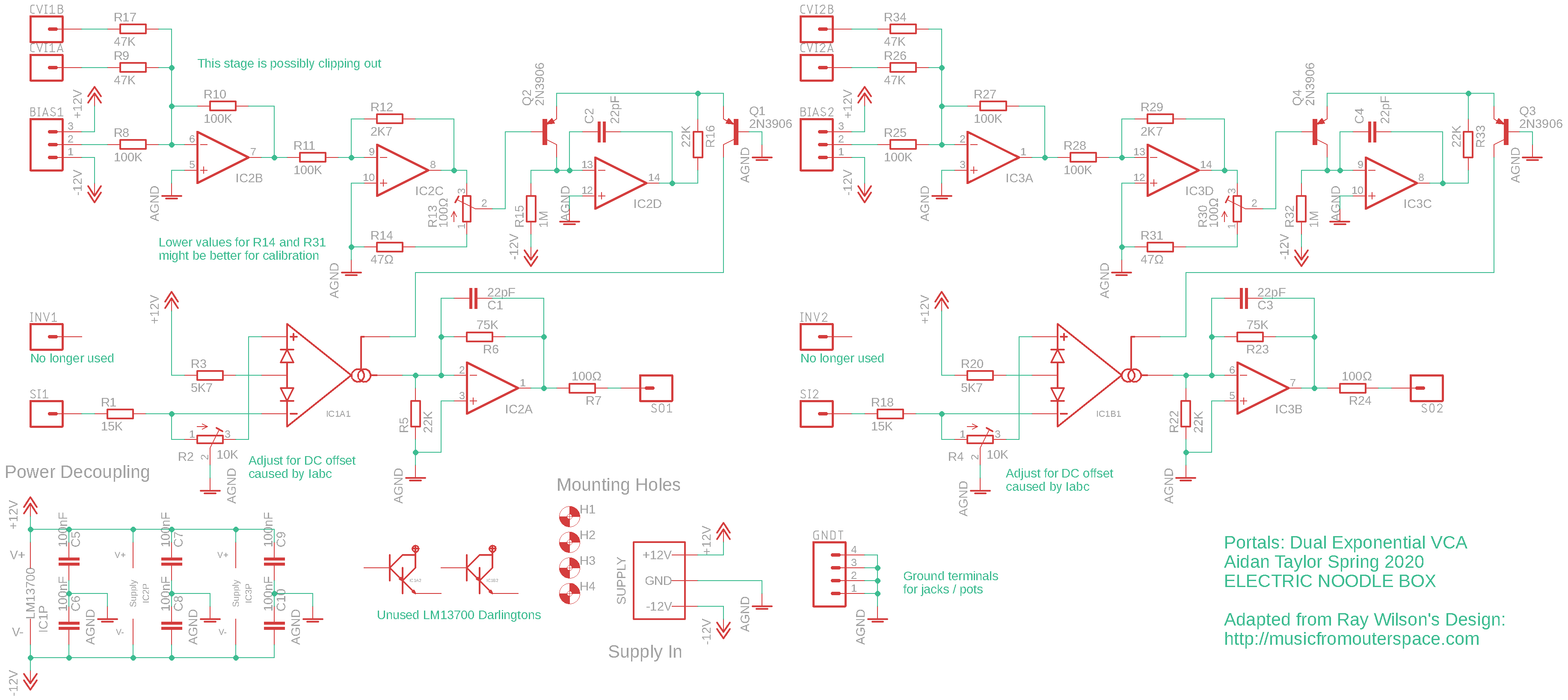
This page describes a DIY Voltage Controlled Amplifier project. It’s a simple design almost straight out of the LM13700 datasheet but with op-amp buffers and a linear to exponential control voltage conversion, an adaption from one of Ray Wilson’s old designs. The inputs are DC coupled and the circuit performs well with both modulation and audio signals, VCAs are essential building blocks in any system! This project should be easy to build on breadboard or veroboard, and the parts are easy to source. I would recommend using an oscilloscope for calibration, though a multimeter may just see you through.
A detailed description of how this circuit works is included at the bottom of this page.
You can purchase a good quality PCB from me which has already been tried and tested through design revisions to work as described – coming soon
Hint: right click and select “View Image” to blow up the image, but you might find the link below to be better:
View the schematic in the repository
Specifics:
- Supply Voltage: ±12V Supply
- Supply Current: 25mA +12V rail, 20mA -12V rail
- CV Input: 0 – 10V (negative voltages will not hurt)
- Signal Inputs: ±5V
- Signal Outputs: ±5V
Building
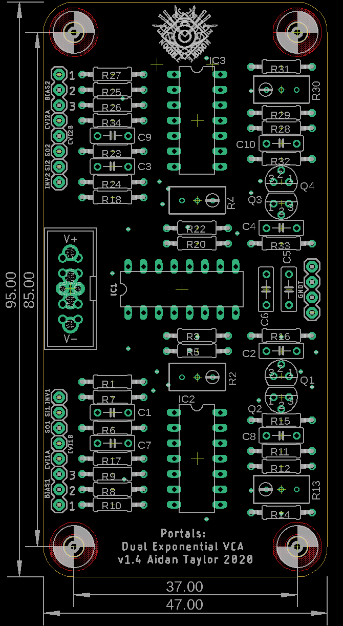
Resistor part numbers are found underneath the part itself due to the limited space on the PCB – use the PCB image below should you need to locate a part.
There is a .pdf with the layout to scale here which also includes the routing on the PCB.
View the bill of materials here
This circuit can definitely be constructed on breadboard for testing, use a full size breadboard and spread out the three chips to allow yourself space to work. You will need a ±12V power supply for testing.
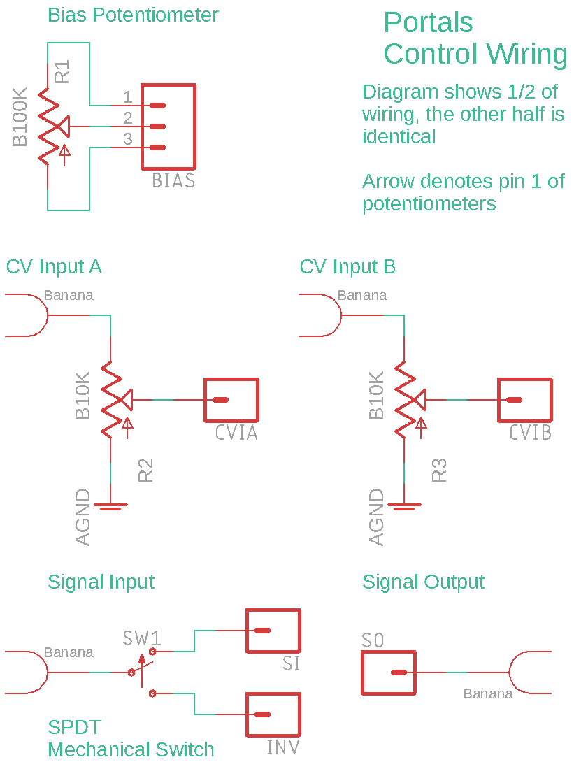
I would recommend using B10K potentiometers configured as an attenuators to ground for each CV input (or at least one on each VCA) – which will allow control over modulation depth. See the image for control wiring (right click and select ‘View Image’ to blow it up):
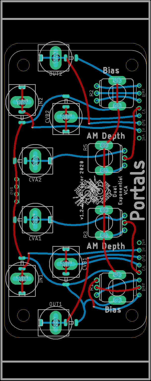
A control PCB and front panel is also available (coming soon) – this is Eurorack panel size standard, and can take either banana sockets or mini-jacks. Be aware that the banana sockets are specifically intended to be Cinch type, as these have a good vertical depth that matches the potentiometers used. The mini-jack footprint is for the PJ398SM (Thonkiconn) sold by Thonk. Link to BOM below.
Layout (to scale)
Calibration
There are two steps to calibrating the VCAs. Trimmers R13 and R30 set the amplifier response to CV input – so will ultimately set the amplitude of the waveform output. Trimmers R2 and R4 adjust DC bias, as Iabc increases (current to the amplifier bias pin of the LM13700), the output tends to get biased with a more positive voltage. Follow the proceedure described below for optimum performance:
You can calibrate the amplifiers by adjusting the two trimmers. Using an oscilloscope for this procedure and a known signal source like 10Vpk-pk (±5V) sinewave is probably easiest if you have the tools available – a stable 5V or 10V DC source would also be suitable. Turn the bias potentiometer fully anticlockwise so the VCA is closed, and apply a 10V DC signal unattenuated to one of the CV inputs. Then connect the oscilloscope to the output and adjust the trimmer until the output is the same amplitude as the input, this means that an envelope or other modulation source at full amplitude will open the VCA to ‘full’ volume. I often find that a smaller resistor is better for R14 to get a better range adjustment from the trimmer – I often opt for 47-100Ω in most designs, which means the trimmer will attenuate more so less current is fed into the transistors. Alternatively, you could also use a multimeter to calibrate – apply a DC signal to the input and using the same procedure as above, adjust the output so the voltage reads the same as the input.
What you will most likely find is that the input get positively biased as Iabc increases, so it is best to adjust R2 and R4 when the amplifier is at full volume, and it is most easy to adjust this bias by monitoring the output on an oscilloscope. When the amplifier is closed it will return to 0V, or very close to ground.
If you are in a pinch and don’t have the tools available, you can probably use your ears to get reasonable VCA behaviour!
Circuit Description:
The LM13700 is one of the best chips still available for building electronic instruments because it is a package with a pair of current controlled gain cells, a key ingredient in VCAs, VCOs and VCFs. It is still actively in production by Texas Instruments and is fairly low cost. They are also easy to understand and have a comprehensive datasheet with lots of nice examples. The basic operation is to use the ‘amplifier bias pin’ which is referenced to the negative supply. Connecting a current source to this pin allows you to adjust the amplifier gain over an input range of 0 to 2mA.
I recommend that you keep the schematic to hand so you can follow this description.
In this design the LM13700 will amplitude modulate the signal that is present at one of the amplifier inputs, applying a signal to the ‘SI’ input will reproduce the waveform in phase at the output, but you can also get a 180º inversion by applying the signal to the ‘INV’ input. The output of the LM13700 is high impedance, considered as a current, so needs to be suitably buffered before linking to something else. The LM13700 includes Darlington NPN buffers for this purpose but using them will unfortunately result in a DC offset at the output thanks to the transistor Vbe ‘diode drop’ effect. You can AC couple the output with a capacitor to block this DC shift, but then the amplifier will not translate DC signals so well. A better option is to use an op-amp with high impedance input like the TL08* series which have JFET inputs – this is the choice in this design.
Overloading the input to the LM13700 will result in non-linear distortion, so in this design each input has a voltage divider (R1 and R2, R35 and R4 on VCA 1). The intention is for one input at a time to be used for the incoming signal. Each input could be broken out to a connector, or alternatively one connector and a mechanical switch could be used to select between inputs. The other input should be left floating in either case, it will terminate to ground via R2 or R4. The input signal should not normally exceed a few millivolts otherwise the amplifier will quickly distort, but signals with larger voltage swings can be connected to the LM13700 by utilising the ‘linearising diodes’, this is the purpose of R3 which will draw about 2mA from the diode bias pin. R5 sets the voltage swing of the output signal, you could substitute this resistor to get a different level if you wanted.
The voltage control is processed through a couple of stages starting with the inverting summing amplifier IC2B. This has connections for two CV inputs which can be used for envelopes and modulation. I would recommend using a passive attenuator in front of the CV inputs made up by a potentiometer to ground (see the control diagram below). Terminals for a potentiometer are also included which allows you to apply a bias to the control signal. If you want to use the VCA with an envelope for dynamics control, then you will probably want to set the bias fully anticlockwise. If you want to use the VCA for ring modulation then you probably want to set the bias to about half way. Otherwise, the pot can be used as a volume control.
The last op-amp in this chain (IC2D) handles the linear to exponential conversion. Q1 is a current source for the LM13700 amplifier bias pin, the base of Q1 is connected to ground, so Vbe is set by the changing voltage at the emitter. Current in BJT transistors is exponentially proportionate to the base emitter junction. Vbe is sensitive to changes in temperature, so Q2 and the accompanying op-amp circuit is designed to compensate for this. Q2’s base is the main voltage input to this section. Q2’s collector is kept at a lower voltage to the emitter and base by R15 which is tied to the negative rail, adjusting the base voltage will proportionately change the current flow. This will ultimately also set Q1’s current and the amplitude of the VCA. The op-amps inverting input is also pulled low by R15, making it lower in voltage than the non-inverting input which is fixed at 0V, so the amplifier will output a current to try and balance out. As Q2’s emitter is connected to the amplifier output through resistor R16, a constant current is placed across Q2. Changes in temperature that effect Q2’s Vbe will be adjusted for by the op-amp, and as Q2 and Q1 have emitters tied together, both transistors benefit from this compensation. Further compensation against ambient temperature using a ‘tempco’ resistor is not worth the added cost (and sourcing of a hard to find part) in this case as it will only compensate against gradual drift, and this will be undetectable to the ear – if you are looking for more scientific accuracy then you might consider changing R12 to be a ~2K7 ~3300ppm tempco.
Initially I thought matched transistors would not provide a significant benefit, but on testing this design (and learning more about how a compensated log converter works) I found that unmatched transistors can result in noticeably skewed volume transitions that might start smooth but end with rapid change as control voltage increases. Matched transistors will make a reasonable difference here and on the PCB the pairs are ‘kissing’ to keep them close in temperature.
