
This module is no longer being developed – the main reason I chose not to continue was down to the small signal mosfet driver for the slew being unreliable. I’m working on a new module which includes sample and hold and voltage controlled slew which is much more stable and predictable – and doesn’t use any rare parts – there are plenty of elements to this page which remain relevant however so feel free to dig in!
This page describes a DIY project which builds a multi-function module comprised of a white noise source, analogue sample and hold, and slew processor. Between these three elements there are numerous patching possibilities which can introduce random and chaotic elements to a musical instrument, hence the title ‘Fundamentals of Chaos’.
White noise can be used directly as an audio source or could be used for modulation. Running white noise into the sample and hold will effectively result in a random stepped voltage. The white noise output level is calibrated with a trim potentiometer.
The sample and hold circuit has low droop (explained in circuit description), and can sample up to a rate of approx. 10kHz – it can be used to create stepped waveforms from CV, but can also be used for sample rate reduction effects. The sample and hold accepts an external signal as a trigger, which will be activated by a rising pulse that crosses 2.5V, this means that audio and CV can be used as well as triggers or gates. The first stage of the trigger handler is a comparator, which is connected to a seperate output, meaning that audio and CV signals can also be used to generate pulse patterns to be used for other purposes.
The slew processor is a simple low-pass filter that uses an optocoupler to set the time constant. It has two modes that switch it between ‘slew’ which will slow down sudden CV changes (think portamento), and audible low-pass filtering. Running a random stepped CV output from the sample and hold into the slew circuit will allow you to dial in a smooth randomly changing CV signal. Running white noise into the filter circuit allows you to filter the noise – so there are a number of interesting possibilites available just by patching elements of the module with each other.
A detailed description of the circuit operation is included at the end of this page for those who are interested.
You can purchase a good quality PCB from me which has already been tried and tested through design revisions to work as described – coming soon
Hint: you can right click and select “View Image” to blow it up, but the link below might be better again:
View the schematic in the repository
Specifics:
- Supply Voltage: ±12V Supply
- Supply Current: TBA
- Inputs: Slew input, Sample and Hold and Trigger inputs are full range (typically ±5V or 0 to 10V). Slew CV input should be 0 – 10V, negative voltages will be clipped. All inputs are DC coupled, with the exception of the Trigger in.
- Outputs: Noise is 10Vpk-pk (±5V). Comparator output is a gate signal (0 – 10V). All other outputs will follow their respective inputs.
Building
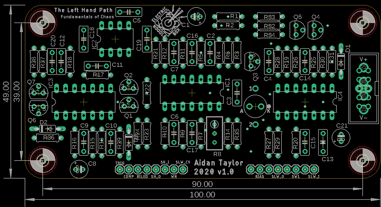
Resistor numbers are found on top of the part due to the small amount of available space, this means that it can be hard to locate a part if you have soldered up the PCB – use the image below to help locate parts.
There is a .pdf with the layout to scale availabe here which also includes the routing map, which might help if you are trying to locate an issue.
View the bill of materials here
This circuit can definitely be constructed on breadboard for testing, you may need more than one full size breadboards, spread out the chips to allow yourself space to work. You will need a ±12V power supply for testing.
See below for control wiring, an attenuator pot (B10K to B100K) should be used for Slew CV input (right click and select ‘view image’ to blow it up):
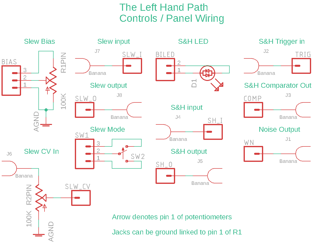
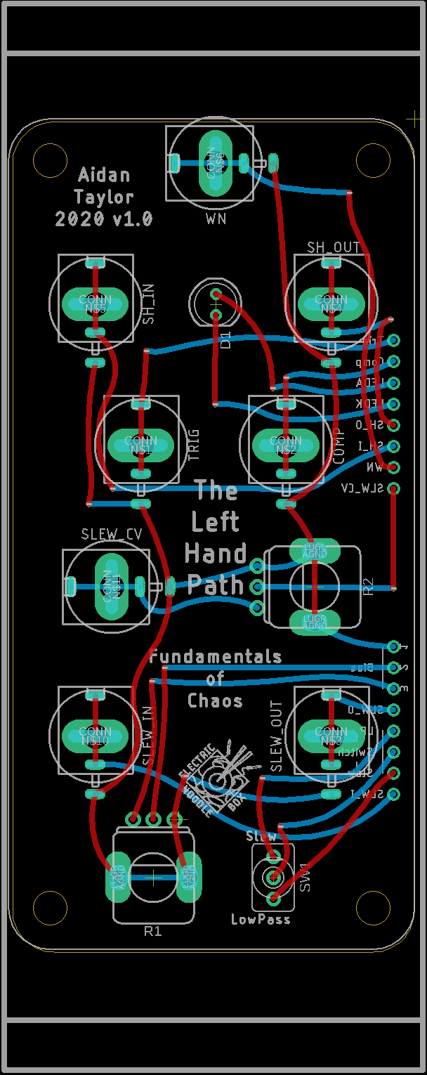
A control PCB and front panel is also available (coming soon) – this is Eurorack panel size standard, and can take either banana sockets or mini-jacks. Be aware that the banana sockets are specifically intended to be Cinch type, as these have a good vertical depth that matches the potentiometers used. The mini-jack footprint is for the PJ398SM (Thonkiconn) sold by Thonk. Link to BOM below.
Calibration
Calibration is simple and just involves adjusting the output level of the white noise source. Ideally, plug an oscilloscope into the noise (Sŵn) output and adjust trimmer R8 to get peaks a little higher than ±5V
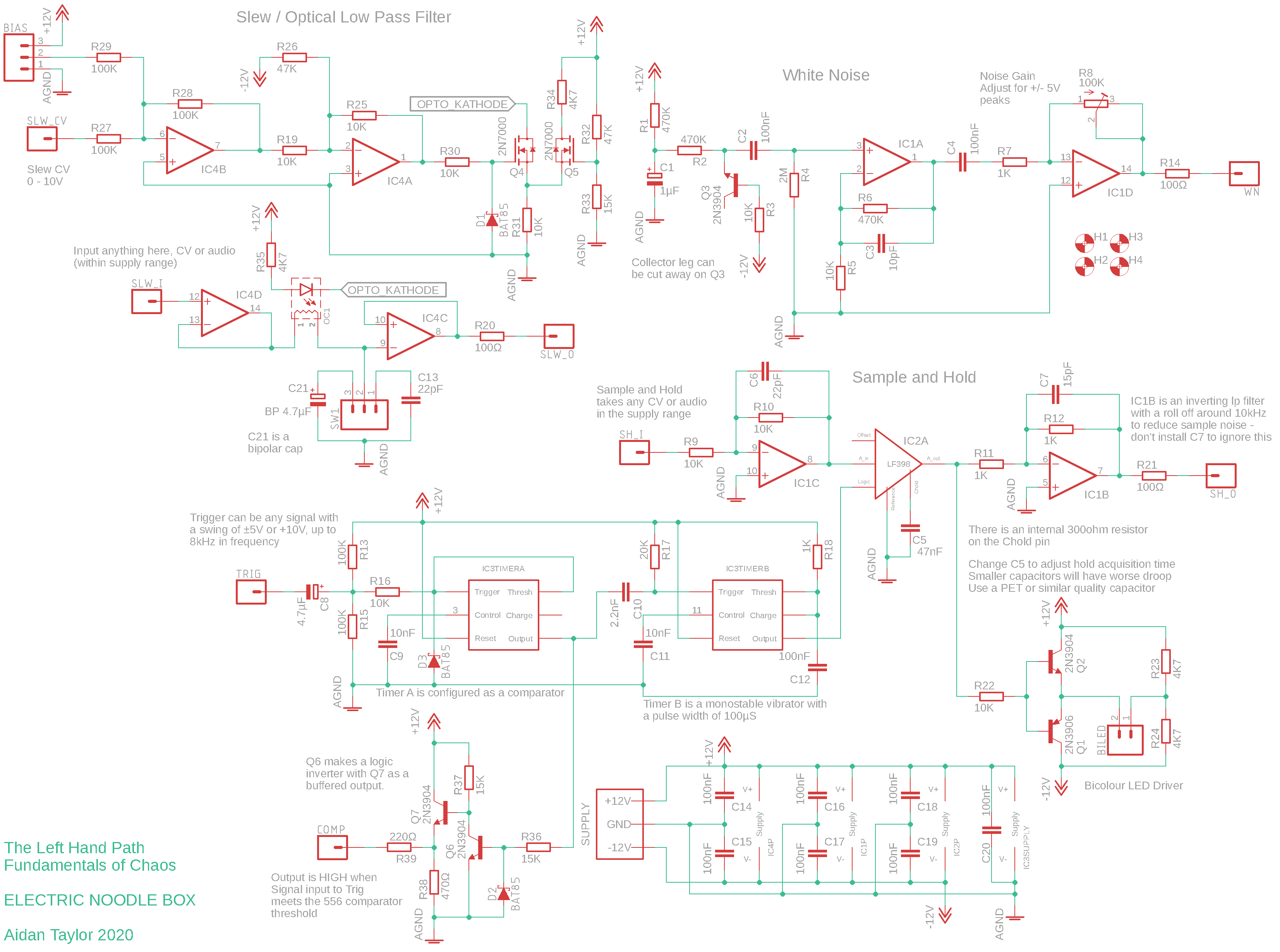
Circuit Description
Each element of this module is described seperately below, and wow there is a lot to talk about here! I would recommend that you keep a copy of the schematic to hand so you can follow the description.
White Noise
The white noise generator is based on the first part of Ray Wilson’s ‘Noise Cornucopia’ schematic, which abuses an NPN transistor! The base-emitter junction is reverse biased, and the collector is unused – I have found a common and cheap 2N3904 NPN produces great results. Wilson recommended cutting away the leg of the collector to avoid it behaving like an antenna – presumably this will result in an audible earth hum like effect. C1 should filter out any ripple from the power supply and C2 and R4 make a high pass filter ahead of the first inverting amplifier stage. I have found that there is a very slight ‘weighting’ towards the negative rail, Wilson’s description suggests that resistor R3 tied to the base of the transistor improves offset – so changing this value might be worth exploring. A trimmer at op-amp stage IC1D will set the amplifier gain before the output. The signal should be adjusted aiming for ~±5V. I find that increasing the signal a little above the ±5V spec was a little better for getting a good range when patching the noise source into the sample and hold sampling input.
Sample and Hold
The sample and hold circuit is based on the LF398 monolithic sample and hold chip manufactured by Texas Instruments and largely follows the application described in the datasheet. A sample and hold circuit typically works by having a junction that either allows a signal to flow when in sample mode, or blocks it when in hold mode. Between this junction and a buffered output amplifier is a charge/discharge capacitor which will hold the DC level the signal was at when cut off (thanks to the output being significantly buffered). A nice example that might make this a little easier to understand can be found in the datasheet of the LM13700 (see the Sample and Hold example on page 24, though without modifications this example won’t work anywhere near as well as the LF398 – something to discuss another time!). If circumstances were ideal, the output amplifier impedance would be infinite and there would be no parasitic leakage into the junction or through the capacitors own equivalent series resistance (ESR), so the charge capacitor would hold the DC level perpetually – but this is never the case, the capacitor will slowly return to a nominal state. As mentioned, in sample mode the input signal flows freely and this will be passed directly to the output – so typically the sample period is very short. The name of the game is finding a balance so that the sample acquisition time is long enough for the capacitor to charge, but not so long that the input signal is passed to the output which will produce audible glitches. Smaller capacitors will charge faster which means the sample acquisition time can be faster, but will also discharge or ‘droop’ at a faster rate. There is a trade off between sample acquisition time and droop in any sample and hold circuit. A final note here is that different capacitor material types have very different ESR ratings, I tend to opt for PET types in any application that requires stability and near-ideal performance. The front page of the LF398 datasheet has a plotted chart showing approximate sample acquisition time vs choice of charge capacitor.
In this design, unity gain inverting amplifier IC1C acts as a buffer and feeds the input signal to the LF398. C5 is the charge capacitor, which should be a 47nF PET type. The LF398 datasheet states that the sample acquisition time should be approximately 100µS, which means the upper sampling frequency is around 10kHz. I have found this value to be a reasonable compromise between acquisition and droop.
To set the sample acquisition time a 556 timer chip by is used, which is two 555 timers in a single package (one of the most popular ICs in electronics history!). The first half of the 556 (IC3TIMERA) is configured as a fast comparator (note there is no charge capacitor in this application). The trigger input is AC coupled which helps to pull audio signals into a more useful range. Resistors R13 and R15 essentially set the comparator threshold. I found programming the comparator a little complex but the network made up by C8, R13, R15 and R16 produced good results, with the switching threshold set at about 2.5V. Note that the comparator output is inverted, the off state is HIGH and the on state is LOW. As mentioned at the top of this page, the comparator output is broken out, and to make it more useful as a gate it is re-inverted by Q6 which is configured as a NOT gate, and buffered with Q7 configured as an emitter follower. IC3TIMERA is followed by the other 556 half (IC3TIMERB) which is configured as a monostable vibrator, which is a very typical use of the 555. In this configuration, the timer will output a pulse with a fixed duration in response to a falling edge at the trigger input. R18 and C12 are used to program the pulse duration, and in this case we are aiming for the sample acquisition time of 100µS. Which is conencted to the logic input of the LF398 – Voila! I strongly recommend checking out the 555 timer datasheet by TI and the 555/556 application notes by Philips should you want to learn more about this useful little chip. I also like the short textbook “Timer, Op-Amp and Optoelectronic Circuits and Projects” by Forrest. M. Mimms III
The output of the LF398 is connected to IC1B, and op-amp configured as a DC integrator. Capacitor C7 in the feedback path will have a linear slew effect – the slew time can be calculated with an RC time constant (made up by R11 and C7) which should be close to 100µS, matched to the sampling time correct ‘noise’ during sampling.
The output of the LF398 is also linked to a transistor push-pull amplifier that drives a bicolour LED.
Slew and Filter
The final section of this module is an almost simple Slew circuit, the signal processing is simple, but the circuit became a little complex when I added voltage control. Slew circuits can be used to smooth hard transitions, they can be used for portamento and other sliding effects. As a signal processor, the circuit block is comprised of a pair of unity gain voltage followers, IC4D and IC4C for buffering the input and output and an RC element inbetween (essentially a low pass filter, if you do a web search on op-amp active low pass filter you should be able to spot the basic elements with ease). I originally designed this circuit to process CV alone, OC1 was a potentiometer which controlled the current flowing into C21, which would charge or discharge from ground in response. C21 was sufficiently large to mean that the charge time could be anything from near instant to several seconds. A good online tool to calculate and understand this behaviour is the Digikey RC Time Constant Calculator.
I wanted to convert the circuit to accept CV control over slew time and decided to try using an optocoupler to achieve this. An optocoupler is simply an LED kissing a light dependent resistor (LDR) in a sealed package that blocks out external light – by modulating the LED brightness you effectively get a voltage controlled resistor – so the optocoupler can make the ‘R’ of an RC filter. When the LED is dark the LDR will have very high resistance, and when lit the LDR will have very low resistance. They are not as easy to source as you might like, many synth DIYers like the Excelitas “Vactrol” series, but these are long obsolete and hard to get. Luckily, this circuit is based on a component that is still well stocked by Farnell, the NSL-32 by Silonex. Optocouplers will have wide tolerence ranges so they are not the choice for a precision circuit, and this is not the intention here. The NSL-32 has an on resistance of approx. 500Ω and an off resistance of 500K.
When designing this circuit I found that R was unhelpfully non-linear and followed a logarithmic curve, which makes sense as perception of brightness or light energy is similarly non-linear. The resistance would also suddenly shoot from a couple of hundred kiloohms to several megaohms between ‘dim’ and ‘dark’ which I didn’t like. I spent some time working on CV control, trying to introduce a DC offset to avoid this, but ultimately I found this non-linearity very unhelpful. So, I began thinking about using an anti-log driver to counter this curve. There are many examples online that use PWM and software for linear LED fading, but I eventually found a circuit that exploited the ‘square-law’ relationship of Id and Vgs in FET transistors that looked like it would be straightforward to adapt for CV control. I tested the design using a pair of 2N7000 small signal FETs, a standard illuminating LED and op-amps for CV and bias control. I found that visually this worked well, and when I swapped the illuminating LED for the opto-coupler, I was able to dial in a lot more control over R with small changes. The driver circuit is comprised of IC4B, IC4A, Q4, Q5 and associated circuitry. IC4B and IC4A are inverting op-amps which accept incoming CV, summed with a potentiometer for bias control. IC4A has a DC offset of about 2.55V which is set by R26. This seemed to be a good voltage to set the ‘dim’ resistance level, R26 may benefit from being a trimmer. D1 will clip negative voltages below -0.7V, to prevent damage to the 2N7000. R35 also limits current through the optocoupler LED – this could be another resistor to adjust for optimisation.
At some point when designing this circuit, I realised that as an RC element was present, it might be interesting to switch the charge capacitor with a smaller one so the circuit could operate in the audio range as a low-pass filter. I tested this using a 22pF capacitor and used white noise and pulse waves as test signals – to my delight this sounded great, with a lovely bit of harmonic ‘growl’ – so it wasn’t hard to make the decision to include this! There was a further pay off as well, which comes from an interesting property inherent to optocouplers, which has been exploited by electronic instrument makers for decades: light memory. Light memory describes LED behaviour where the switch on time is very fast, instant as far as perception is concerned, but the switch off time is comparatively slow. In optocouplers this can be anything up to a number of seconds, the NSL-32 datasheet states that the decay time is 500mS. The dynamic response of the optocoupler is similar to that of a guitar string being plucked or a drum being beat – so when an optocoupler is utilised as a control element in a VCA or VCF, the dynamics behaviour can sound a lot more natural than electronics do typically. Buchla and Serge in particular made extensive use of this in their electronic design.
