
This page describes an electronics project to build a analogue ‘clock’ generator for musical timing. A clock module in synthesizer systems will generate periodic pulses which can be used for applications such as incrementing sequences, triggering sample and hold or triggering envelopes. The design is a hybrid analogue and digital circuit that has an ATTiny85 MCU at its heart. A potentiometer sets the overall frequency or BPM of the clock which is output to a patch point. Four divisions of the clock frequency are also provided, / 2, / 4, / 8 and / 16. A sixth output is provides randomly generated looping gate or trigger patterns over a measure of 4 beats, which can be used to create interesting rhythmical phrases with modules like Knives. The control voltage input will modulate the clock frequency which is scaled exponentially in the software, which can be used to create drifting organic timing. Buttons are provided for randomising the pattern and starting/stopping the clock and CV / trigger inputs are provided for clock modulation, and clock start/stop. Holding down the pattern button selects between gate and trigger modes for the 32 step sequence. LEDs can be included for all pulse outputs.
Code is provided and a detailed circuit description can be found at the bottom of this page.
You can purchase a good quality PCB from me which has already been tried and tested through design revisions to work as described – coming soon
Hint: Right click and select “View Image” to blow it up, or alternatively follow the link below for best quality:
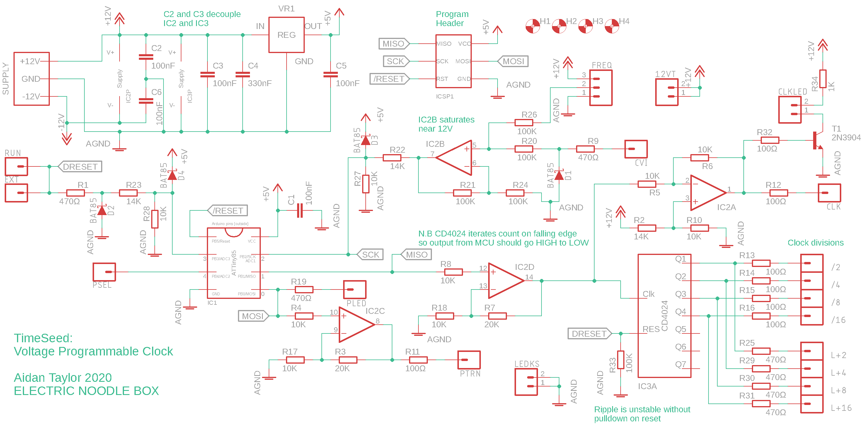
View the schematic in the repository
Specification:
- Supply Voltage: ±12V, there is a localised +5V regulator for the MCU
- Supply Current: 100mA +12V rail, 10mA -12V rail (LEDs, MCU and regulator all load the positive rail, increasing the LED current resistors R19, R25, R29, R30, R31 and R34 might improve current draw at the expense of LED brightness). Be aware that the pattern LED is driven with 5V, which is half the voltage of the other LEDs so resistor R19 should be ~1/2 the value of the others selected.
- CV Input: 0 – 10V (avoid negative voltages, clipping is included in the circuit to avoid damage)
- Clock, Division and Pattern Pulse Outputs: 0V off, 10V on
Building:
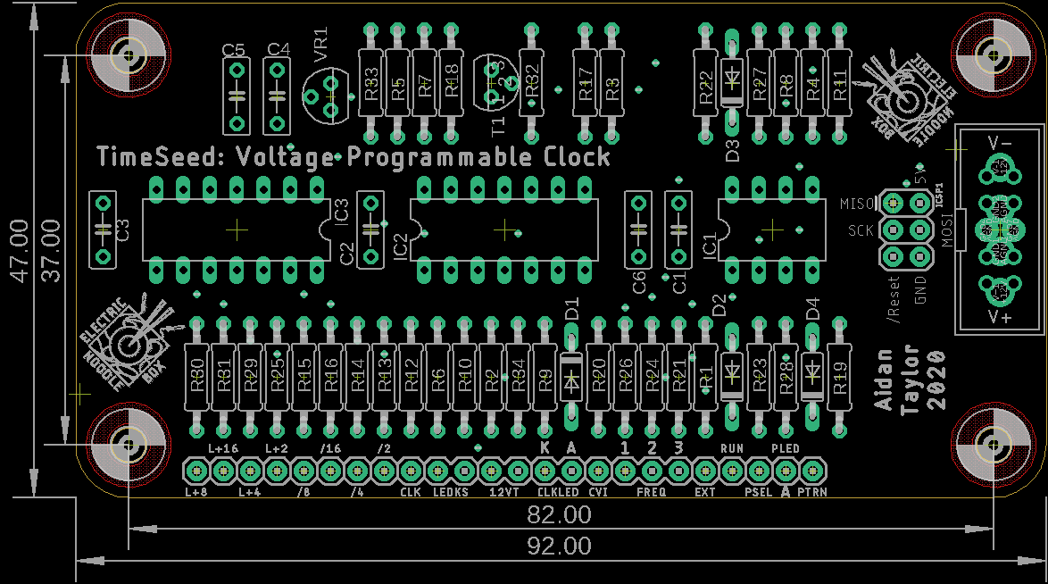
Resistor numbers are found on top of the part due to the small amount of available space, this means that it can be hard to locate a part if you have soldered up the PCB – use the image below to help locate parts.
View the bill of materials here
This circuit can definitely be constructed on breadboard for testing, use a full size breadboard and spread out the three chips to allow yourself space to work. You will need a ±12V power supply at very least for testing, and having an Arduino Uno handy will make flashing the MCU straightforward.
If you are wiring to a panel, I would recommend including a 10K – 100K potentiometer configured as an attenuator to ground for the incomming CV signal, this will act as a modulation depth control. See below for control wiring (right click and select ‘view image’ to blow it up):
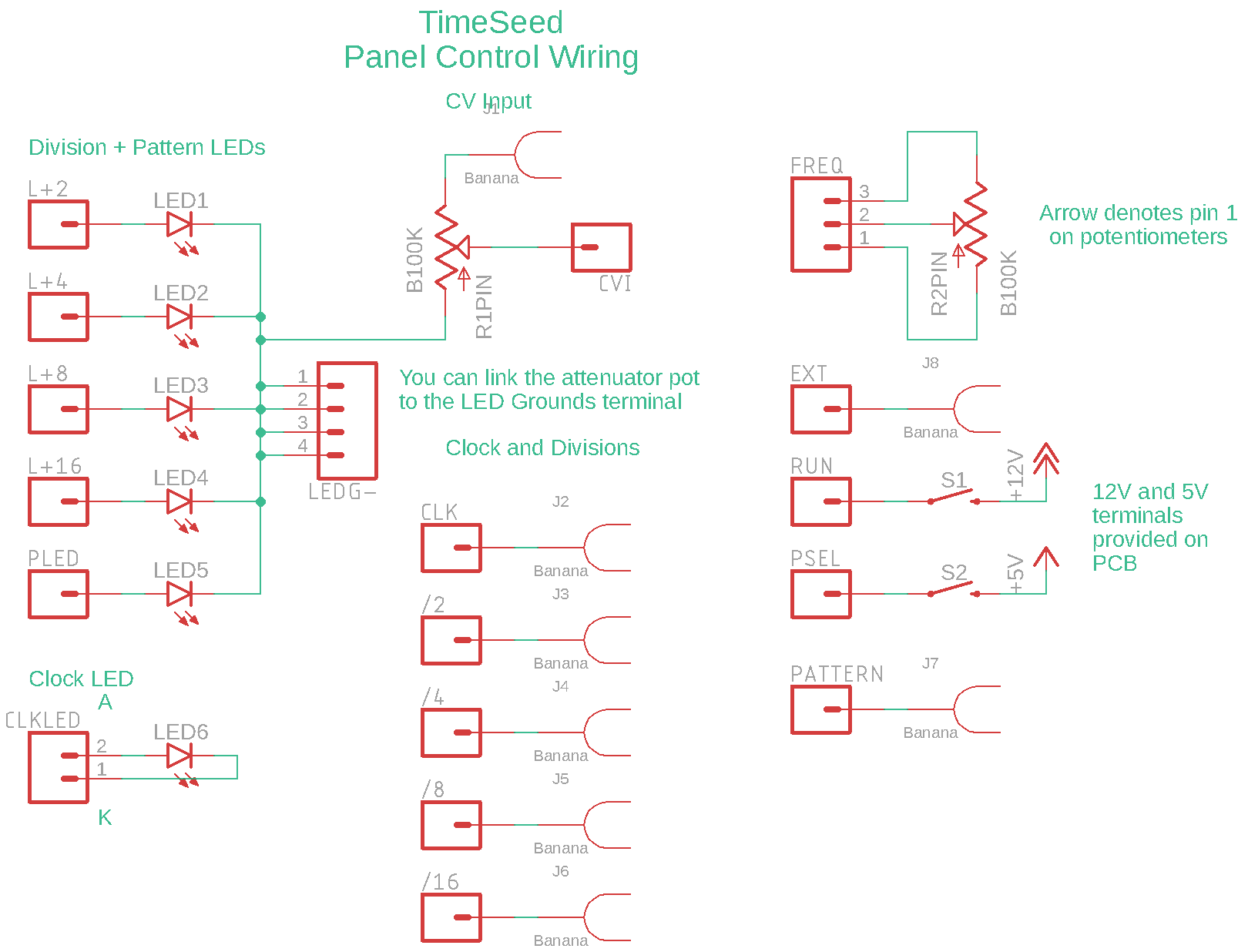
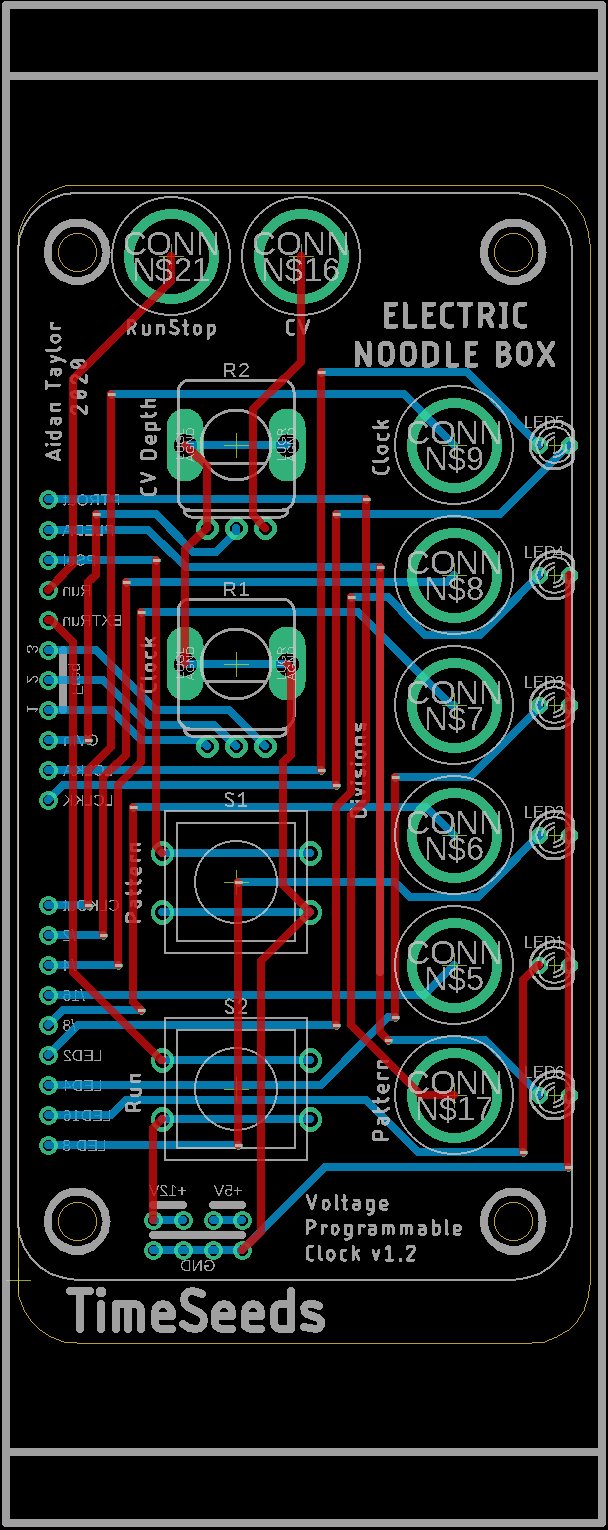
A control PCB is also available (coming soon) – this is Eurorack panel size standard, but uses banana jacks.A control PCB and front panel is also available (coming soon) – this is Eurorack panel size standard, and can take either banana sockets or mini-jacks. Be aware that the banana sockets are specifically intended to be Cinch type, as these have a good vertical depth that matches the potentiometers used. The mini-jack footprint is for the PJ398SM (Thonkiconn) sold by Thonk. Link to BOM below.
Layout (to scale)
Code:
Code can be found in the repository by following the link below, it is well commented. To keep flashing relatively simple, I created the firmware using the Arduino IDE. You can either compile it using the Arduino IDE or you could use something like PlatformIO, Arduino is the simplest option.
View the source in the repository
Flashing:
A breakout header is provided on my PCB which matches the Arduino style ISP (in system programmer) connector. The easiest way to flash is to have an Arduino Uno (or a similar model) to hand and some jumper leads, the Arduino will be used as a programming interface, an example sketch is provided with the Arduino IDE which needs to be loaded onto the Uno (see File>Examples>ArduinoISP). You will also need SpenceKonde’s ATTinyCore installed.
In the Arduino IDE, flash the Uno with the ArduinoISP sketch. Then, go into Tools and set the following:
- Board: ATTiny85/45/25
- Chip: ATTiny85
- Clock: 8MHz (Internal)
- Programmer: Arduino as ISP (ATTinyCore) Don’t forget to change this back later on!!
Connect the Arduino Uno to the PCB, soldering a pin header will be helpful here. I have a homemade pogo pin header for doing this. A guide for wire connections and programming can be found here
Before you ‘flash’ the chip with the sketch, make sure you ‘Burn Bootloader’ – you only need to do this once and it will configure things like the clock fuses on the ATTiny85. Once you have done that you can go ahead and flash the chip.
Circuit Description:
The circuit is comprised of three chips, the ATTiny85 MCU, a CD4024 CMOS binary ripple counter for divisions and a TL084 for voltage processing.
The MCU acts as the brain in this design, reducing the need for a series of logic chips. Clock frequency control is set by the ATTiny85 ADC input on pin 7. IC2B is a non-inverting summing amplifier, which sums the incomming modulation voltage with the clock frequency potentiometer. The incomming modulation voltage is clipped with D1 to prevent it going negative – the diode drop will mean that the voltage can go as low as -0.7V – this is too low for the MCU as the datasheet specifies that the pins should not go lower than -0.5V in the maximum ratings, but we should be fine because the voltage divider made up by R22 and R27 should mean that the voltage will never be lower than 0.292. The diode D3 is also a clipping diode which should prevent the voltage going higher than 5.3V, which is within the MCU pin maximum rating of 5.5V. A similar clipping circuit is employed for the Run/Stop control, a button is tied to 12V and is linked with a patch input, which is expecting a 0-10V pulse input. D2 again should clamp voltages to go no lower than -0.7V if an undesirable signal is input, and the voltage divider made up by R23 and R28 should set the lowest voltage to -0.292 and the highest voltage to around 5V. As a failsafe, D4 should clamp the incoming voltage to go no higher than 5.3V. An incoming pulse will reset the CD4024 sequence, I found this voltage needs to be higher than 5V for the CD4024 to register it, so the input is taken directly before the voltage divider. Two outputs from the MCU are used for the Clock and Pattern outputs. The pattern output has an LED directly attached as the MCU can output up to 40mA per pin, and the output is buffered and boosted from 5V to 10V by non-inverting amplifier IC2C. The Clock output is inverted, that is, the active clock is output at 0V and inactive at 5V. This is because I found the CD4024 is iterated on a falling edge pulse which meant the divisions were always half a beat out of step. IC2D is a non-inverting amplifier that boosts the 5V signal to 10V for the CD4024 input. IC2A is a unity gain inverting ampifier which is also linked to the output of IC2D, this amplifier has a reference bias of 5V set by the voltage divider made up by R2 and R10 and as such it will invert the clock pulse for external use. An LED is connected to the output of this amplifier, buffered with T1 to prevent overloading amplifier.
The CD4024 uses the 12V supply which means the outputs are suitably high for direct use, and as outputs are all buffered, LEDs can also be directly connected. The CD4024 is a 7 stage binary ripple counter, but only the first four stages are utilised in this design. The outputs activate and deactivate as divisions of the incomming clock signal, so the first four grant divisions of 2, 4, 8 and 16. A high pulse to the reset pin will reset all counting, I found that this pin needs a pull down resistor or the IC counter tends to start doing odd things.
Everything else is handled in the code. A breakout ISP header is provided for flashing the MCU, this can easily be achieved using an Arduino Uno (and some other models) as an ‘In System Programmer’ so this module can be hacked if you can think of other functions you might like. I use SpenceKonde’s excellent ATTinyCore and the Arduino language to program, which can all be done in the Arduino IDE.
