
This page describes a DIY project for a multi-purpose function generator module. This module produces waveforms in response to the input and has a variety of modes: an attack-release (AR) envelope which is triggered by the signal input crossing a threshold voltage, an envelope follower which will behave like a voltage controlled slew, and will produce an AHR envelope in response to a gate input, and a self-looping ramp generator. Each mode produces a linear up and down ramp which have individual voltage control, and can be trimmed to track 1v/Octave which should allow the waveform to track musical notes over at least a few octaves range. I haven’t seen a design quite like this, my inspiration was the Serge Universal Slope Generator, and while Transients is less featured than the USG, I believe my circuit is simpler – I was surprised my approach worked so well when I tried it!
How to set the modes:
- Press the ‘mode’ button for AR (attack, release) envelope mode. A gate or signal input will cause the envelope to complete a full single cycle
- In AR mode, press the ‘loop’ button for LFO mode. The LFO is effectively a looping AR envelope which restarts once the release phase is complete
- Depress the ‘mode’ button for Slew and Envelope Follower mode. This mode is highly dependent on input. A gate signal can be used as an input to make an AHR envelope (attack, hold, release), the module will ramp up in response to a HIGH gate, and hold in the HIGH state, at any point it will ramp back to zero if the gate goes LOW. Any other signal input will cause the module to track the voltage like an envelope follower, the up / down ramp controls add a slew effect to the tracking.
Note that increasing the CV voltage applied to the inputs will result in slower ramps. If you would prefer the LFO to behave more traditionally (increase in frequency with voltage), you will want to invert your CV signal.
This circuit is capable of producing a variety of modulations for a modular system, including fast dynamics and slow transitions, so it is an invaluable addition. This is a slightly advanced DIY project, but not unsuitable for beginners, some additional tools are needed for good calibration.
A detailed description of the way this circuit works is included at the bottom of this page.
As there is just a little too much circuitry to squeeze into my normal module form factor (100x50mm), I made this into a dual module – and besides, you are going to need a modulator for your modulator right!
You can purchase a good quality PCB from me which has already been tried and tested through design revisions to work as described – coming soon
Hint: You can right click and select view image to blow it up. The full schematic for a dual module can be found in the repository here
Specifications
- Supply voltage: ±12V (on board +/- 10V reference included)
- Supply current: TBA
- Signal inputs: Gates and triggers are typically 0-10V, the switching threshold is less than 5V so 5V triggers will work. Audio signals are typically ±5V (10Vpk-pk)
- Signal output: Envelope/LFO 0-10V, slew/envelope follower will follow the input signal and can go into the negative range.
Building
There is a .PDF file with the layout to scale here which also shows the copper routing if you run into problems and want to check.
View the complete Core Bill of Materials here
This circuit can be constructed on breadboard for testing, use a full size breadboard and spread out the components to allow yourself space to work. You will need a ±12V power supply for testing.
A control PCB and front panel is also available (coming soon) – this is Eurorack panel size standard, and can take either banana sockets or mini-jacks. Be aware that the banana sockets are specifically intended to be Cinch type, as these have a good vertical depth that matches the potentiometers used. The mini-jack footprint is for the PJ398SM (Thonkiconn) sold by Thonk. Link to BOM below.
Calibration
There are 6 trimmers to calibrate the dual module, 3 for each channel. Using an oscilloscope is the best option for calibration. If you don’t have one, maybe check if you have a local Makerspace or Hackspace where there will undoubtedly be an electronics setup. Calibrating for 1v/Oct (or technically -1V/Oct) is possible in theory, but I haven’t tried to do this accurately – instead I have concentrated on getting ramps to change at ‘close to an octave’ per volt – I think getting perfect accuracy would be tedious and without much point!
First, press the mode switch in so the channel is in envelope follower mode. Set the attack release controls fully anti-clockwise for the fastest ramp time. Apply a fixed signal to the input of the module, the output should ramp up and down in response. Use a scope to monitor the input and output from the module and adjust the gain trimmer (R3 or R32) to the output to match the input. You should also be able to do this with a fixed DC signal as an input, and use a voltmeter to check the input matches the output.
For 1v/oct tracking, depress the mode switch and activate looping by pressing the loop switch in. Turn the CV attenuators to fully clockwise (maximum) and connect a known source of CV or a stable DC signal. Connect your oscilloscope to the output of the channel. Keep in mind that the module will track over a particular range from a centre point, the further away you get from the centre, the less accurate the tracking will be, but in perfect conditions, you should be able to see the ramp time double for every volt applied to the CV input. I calibrate one ramp at a time, so either up or down. To calibrate the up ramp time – turn the down ramp control fully counter-clockwise so it is fastest and turn the up ramp control up so you can count the ramp time across a couple of the horizontal devisions of the scope (I worked to 2ms divisions and 8ms ramp time at 0V CV). When you add 1V of CV, the ramp time will increase, the aim is to calibrate so that the ramp time is double, so it will take twice as many horizontal divisions to complete. Adjust the up ramp trimmer to calibrate to this effect. The up ramp time is calibrated with R9 for channel A and R37 for channel B, the down ramp time is calibrated with R19 and R45.
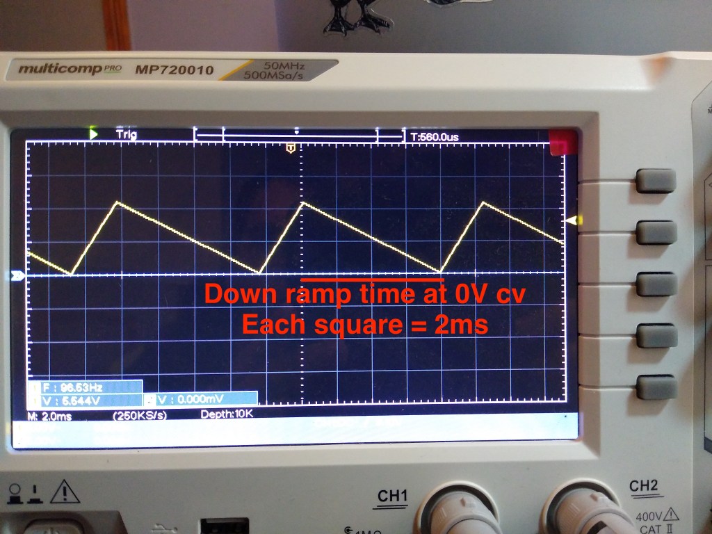
Note in this image I was calibrating the down ramp time. Each horizontal division on the scope view is representative of 2ms, I have dialled in the down ramp using the panel control so that it lasts 8ms. I would expect 1V of CV to increase this time to 16ms.
Some tips here:
- When calibrating for the up ramp, set the scope to falling edge trigger, that way the resulting waveform won’t move on the scope when you adjust the up ramp time. When you are calibrating the down ramp, set the scope to rising edge trigger.
- You can normally adjust the horizontal position on a scope as well, which might make things easier.
- When you adjust the trimmer, you will find that ramp time changes for CV at 0V and CV at 1V. It is best to change things gradually and keep checking the effect as you go.
Circuit Description
I recommend you keep a copy of the schematic to hand to follow along with this description.
This is yet another excellent LM13700 circuit – if I am allowed to say so! A number of my circuits have a very similar configuration where the current output of the LM13700 is fed into a high-impedance buffer (an op-amp in voltage follower configuration), with a capacitor to ground in between. The output from the op-amp makes a negative feedback path back to the LM13700, which when calibrated will keep the resulting signal very stable; you can think of the current output from the LM13700 as being a tap which is sourcing/sinking current from ground via the capacitor, adjusting Iabc (the LM13700 gain control) will adjust current meaning the capacitor will charge and discharge faster/slower, and you can effectively close the tap so the capacitor holds a voltage thanks to this negative feedback path. A suitably high-impedance input matched with a suitably low-leakage capacitor means that the voltage output from the op-amp will be held almost indefinitely with very low ‘droop’ (the capacitor will discharge to 0V somehow, so the trick is controlling this as much as possible).
As I was working on a voltage controlled slew design, I began to wonder if it were possible to have seperate controls for both the up and down envelopes, and it turns out this is actually surprisingly simple. I have used diodes in a number of designs to control the flow of current down two separate signal paths, and that is the key to this design. Two halfs of an LM13700 are used (IC1A1 and IC1B1) and connected to the same op-amp (IC4A) and capacitor (C1), but each LM13700 is followed by a series diode (D1 and D2). The two diodes face opposite ways to each other, which effectively funnels positive going current through one amplifier, and negative going through the other. C1 should be a good quality, low leakage capacitor for good performance, I choose PET types like WIMA brand. IC1A1 and IC1B1 have gain set individually via their amplifier bias pin, which means you can tap the flow of current in either direction. Input CV is connected through a linear to exponential converter that I use in a number of my circuits (see IC3B and IC3A), Q1 and Q2 are matched as are the transistor pairs in each CV processing section (this circuit is explained in Prism if you want to understand it further) – note one difference here from my other designs, the output from IC3B connects to the base of the servo transistor, instead of the current source transistor – this means Iabc decreases when the input CV increases, resulting in slower ramps, slower LFOs or ‘more slew’.
The ramp output of this circuit block is a linear slope as a result of the negative feedback loop set by R4. Also notice that the LM13700 inputs are in parallel, and only one trimmer is needed for calibration – simple and amazing!
This circuit has another chip to allow it to do some interesting things, this is a CMOS dual flip-flop called the CD4013. Flip-flops are typically used in logic circuits to store a single bit of data, and I thought this might be helpful in a resetable envelope configuration. I admit, I find that following the logic of a flip-flop is quite hard to follow, and it did take me some time with trial and error to get this circuit working correctly, but the results are good. Maybe it is best to explain the operation as a set of events, consider the LM13700 and op-amp section as being a circuit block, where the input starts with the LM13700 and the op-amp provides the final output. Also note that the mode switch on the front panel selects the input to the LM13700 between either the external input or the output from the 4013 section.
AR Envelope mode:
With the ‘mode’ switch open, the LM13700 circuit is fed directly from a 4013 logic output. The input signal is connected to a passive high pass filter (R25 and C23) which is followed in series by a transistor buffer. A pulse input will be filtered at ~530Hz and the result is a narrow pulse at about 2ms – this is enough time for the capacitor to charge sufficiently so the transistor buffer switches on, I use one of the spare Darlingtons on the LM13700 for this, D5 is used to protect the Darlington pair from negative going signals. The first half of the 4013 (IC2B) has the Data and Clock pins connected to ground, and the Set and Reset pins connected with pull-down resistors. In this configuration, IC2B’s Q output will follow the Set pin. If the input voltage crosses the 4013 threshold (approx. 6V) then the device is ‘Set’ and the Q output will switch to logic HIGH, and will remain HIGH until the reset pin receives a pulse. The LM13700 circuit will begin to ramp up as it follows IC2B’s Q output. The output of the LM13700 circuit is fed back to R28 and into the Clock input IC2A (the other half of the 4013). IC2A has Set and Reset connected to ground, and the Data input is connected to the /Q output – which means that the stored bit is ‘flipped’ for every clock pulse. The clock is pulsed by a positive edge, so it will detect the increasing ramp of the LM13700 circuit, when this happens, a bit of data is pulsed to the Reset pin of IC2B. This will cause the Q output of IC2B to ‘reset’ and go low, so the LM13700 will follow suit and ramp back down to 0.
There is a little research to put in here, I don’t quite understand why the IC2A section works as it doesn’t have some kind of reset, and the clock should only be triggered by a rising edge. I spent some time planning on using a signal from IC2B to reset IC2A, but everything I tried caused the circuit to lock up – in this configuration it worked and I don’t know why – if anyone can explain in the comments, I am all ears!
Envelope Follower mode:
If the ‘mode’ switch is closed, then the input to the LM13700 circuit is fed directly from the input to the module, which can be either a gate or any other kind of signal. A gate will result in a AHR behaviour from the envelope, as the ramp will rise in response to the gate and will hold at the gate voltage until the input goes low, and will then ramp down. If an oscillating or varying signal is introduced (e.g. an LFO), the LM13700 circuit will do its best to match the voltage of the input, but will adjust more slowly according to the ramp settings, creating a voltage controlled slew effect in this case. Note the fastest ramp time is about 2ms, so waveforms above 500Hz will be significantly effected even at the fastest ramp settings.
Looping mode:
If the ‘mode’ switch is open and the ‘loop’ switch is closed, the AR envelope will cycle. All of the above description for the 4013 behaviour applies, but in addition, a discrete schmitt trigger made up by Q5 and Q6 is added into the loop. Consider the schmitt trigger like this: the output is a logic signal and is the reverse of the input. Q5 takes a signal in and will switch ‘on’ when a threshold is met. Q6’s base is tied to Q5’s collector, so when Q5 switches on, the collector looks a lot like logic LOW, and Q6 will switch ‘off’ (the opposite is also true of course). Q6 is configured as an emitter follower, so the output will follow the switching behaviour and will be suitably buffered.
The input to the schmitt trigger is the LM13700 circuit output, so when the envelope is high, the schmitt trigger is logic LOW, and when the envelope is low, the schmitt trigger is logic HIGH. The threshold is very low, so when the envelope is almost at its lowest voltage, the schmitt trigger sends a HIGH logic pulse out, and is connected back to the ‘Set’ input of IC2B, which restarts the envelope cycle – phew!
